

Solderless breadboards are the fastest and most flexible way to design and experiment. When the circuit is ready for more permanent use, there are several methods of connecting components together that are appropriate for one-time designs in robots:

Completed one-sided circuit board.
Although I eventually want to use surface-mounted components and to make double-sided circuit boards, I decided to eliminate additional new variables for my first attempt. I limited the first project to through-hole components (such as standard DIPs) on a single-sided circuit board.
I’m experienced with through-hole components and I’ve soldered 0.1-inch point-to-point perf boards. I saved myself a lot of trouble and frustration in learning a new technology by building on top of what I already know well.
The chosen circuit isn’t important, although it should be fairly simple for your first attempt. I decided to create a daughterboard that contains complete circuits for a voltage regulator and two DC motor drivers for Sweet, a line-following robot.
This board includes resistors, small DIP sockets, capacitors, a switch, an LED, Molex connectors, diodes, a jumper, and a few crossover wires. An excellent variety of common components with which to experiment!
Before writing this web page, I’d never used a PCB CAD layout program before. I didn’t own any PCB CAD software and I didn’t want to pay hundreds of dollars to buy a package. I searched for 'free PCB software' and found several viable packages. Honestly, unless you need to make a huge board or more than four layers, there are plenty of free programs that work fine.
When trying to design a circuit, I got overwhelmed on the first couple of attempts. I discarded several windows and files. I was trying to make too large of a leap by designing with surface-mounted components, two-sided boards, components on both sides, and very thin traces.

Discarded surface mount layout
To get beyond this mental obstacle, I designed the circuit by physically laying out components on an ordinary perf board with pre-drilled holes every tenth of an inch. Then I copied the patterns into the software and switched back-and-forth as the circuits progressed. On the screen I could see efficient changes, which I then tried on the physical layout. Sometimes I would notice a problem on the physical layout that I needed to correct on the screen.
I worked on a single functional unit at a time (like the voltage regulator) and only proceeded after I had perfected that section. This allowed me to experiment, apply, and learn layout skills without having to go back and throw out a lot of prior work.

Finished circuit
The picture isn’t to scale. The final board is 3.8 inches by 2.5 inches to comply with the size of a manufacturer's PCB service. Of course the software can create other board sizes.
The green lines are copper connections on the bottom (lower layer) of the board. Notice the green text appears flipped since it is being seen through the invisible board.
The red lines and circles (through-hole pads or vias) are on the top layer of the board. Because through-hole components are being used instead of surface-mounted components, each red circle represents a hole that needs to be drilled (ick!).
The yellow lines and text are component outlines that won’t actually appear on the copper of the board. Instead, more expensive boards can be ordered with the yellow portion printed in ink. For my purposes, the yellow is ignored.
The grid (light lines or dots) won’t appear on the copper either. They’re used as on-screen guides for positioning components at tenths of an inch.
Red and green circles appear at all four corners for drilling holes for mounting screws.
My finished layout reflects simple, beginner choices:
 .
Although not technically necessary with such thick traces, I wanted to practice rounding corners
.
Although not technically necessary with such thick traces, I wanted to practice rounding corners  to reduce noise that will occur on smaller, thinner lines.
Here are some additional PCB layout tips.
If you’re going to make PCBs from photosensitive boards, you can print each side directly to overhead transparency film and flip the transparencies as necessary to make the image appear with the correct orientation.
If you’re going to use an iron to transfer the toner to the PCB, be sure to mirror (flip left-to-right) the top layer. This can be done by some printers in Page Setup, some PCB programs in File->Print, or can be captured in a screen shot and flipped in a paint program. The top layer needs to be mirrored because the toner will be mirrored back when ironed onto the board. If this seems strange, just try it and you'll see.
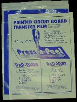

Left: Techniks Press-n-Peel Blue transfer film. Right: Paper and final printout
I purchased a five-sheet package of Techniks Press-n-Peel PnP-BLUE Printed Circuit Board Transfer Film for Laser Printers and Photocopiers. At Electronix Express it costs $9.90 (#03PNPB5). The cost decreases and approaches a dollar a sheet in larger quantities.
After testing the printout on inexpensive plain paper, the circuit should be printed to the dull side of the PnP-BLUE transfer film.
When I first tried making a board, I made a couple of mistakes with mirror images and I made some changes to the circuit. As a test, I cut out the used portions of the blue paper and then re-fed the remainder back into the printer.
Although I can’t guarantee this because it might harm your printer, the final circuit transferred just fine even though the same sheet of blue paper (becoming ever smaller as I cut off the printed portions) had made three passes through the printer. I’ve repeated this technique over the years, and it continues to allow me to reuse the unprinted portions of the sheet, saving money.
As an alternate to Press-n-Peel, many people have had good luck with clear transparency sheets or glossy paper.


Left: Scotch-Brite scour pads and a single-sided copper board. Right: An iron
Plain, copper clad PC board can be purchased from many different retailers. Expect to pay $2 for a 4-inch by 4-inch board.
If you’re using transfer film or press-on labels, then don’t buy pre-sensitized boards. They’re for transferring the image photographically.
Try not to use double-sided boards if only one side is going to have a circuit. The unused copper must be removed by the etching solution. It takes longer to etch and uses up the etching solution sooner if large, unused areas of copper are exposed.
If necessary, cut down the board to the approximate size. A table saw with a diamond blade or a shear are the best choices (MicroMark sells both power tools). However, a Dremel with cut-off blade or a hacksaw works okay. In any case, be sure to wear goggles and a breathing mask.
Always clean the board with water (perhaps some cleaning solution) and a scouring pad. The scrubbing removes grime and oxidation, thus preparing the surface for a crisp transfer and ultimately firm soldering.
After drying the copper board, place the blue transfer paper with the image (toner) side against the copper. Carefully position the image -- the clinging of the plastic to the clean copper helps. Then place a piece of ordinary white paper over the blue paper. (The white paper helps the iron glide without catching or smearing the blue paper.)
Follow the transfer paper’s directions for ironing. Usually a low synthetic to wool setting for a couple of minutes (it usually takes me up to five minutes); no steam.

Left: PCB with pattern incompletely transferred. Right: The film showing the black toner that failed to transfer
Although you want to cover the entire board with enough heat and pressure, the board edges just seem to be the most difficult to transfer correctly. For best results, concentrate the tip of the iron on the outer edges while the rest of the board receives the less intense (but more constant) heat and pressure of the middle portion of the iron. With the iron tip, carefully rub each and every detail that appears near and edge or corner.
In my first attempt, I failed to iron the very edge of one corner of the board. Even the thinnest lines of the middle-located text transferred well, but the missed edges failed to adhere to the board.
Either let the board and blue paper cool off or rinse them in cool water. I tried both methods and they worked equally well (I tend to run the board under water so that I can see the results right away). When the board is cool, slowly peel off the blue paper to reveal the transferred image.
Double-check the inverted image on the blue paper for failed toner transfers. Any failed transfer will appear as black toner remaining on the blue paper. This will be the most common problem encountered.
Also, stop everything at this point and try placing some chips on the image on the board.
Everywhere there is toner there will be copper (after etching). So, if the chips don’t fit, the text is backwards, or the parts aren’t in the expected locations, now is the time to figure out what went wrong and scrub the board clean to make another attempt.


Left: Attempt to restore via and pattern using permanent marker. Right: After etching the marker portion failed to protect the underlying copper
Use a permanent marker or rub-on patterns to replace missing toner. The permanent marker portions must dry for a few hours and usually works better with a second coat. My initial attempt failed as the “wet” marker portions etched away almost as much as the completely exposed areas.

Glass jar of ferric chloride etchant
The etchant is a chemical that reacts with exposed copper and removes it from the PC board. Copper covered with resist (toner, rub-on patterns, tape?, and permanent marker) won’t be removed, although it will begin undercutting if left soaking for too long.
Ferric chloride (iron chloride hexahydrate; ferric trichloride hexahydrate; FeCl3 6H2O) is a popular chemical for etching. So, too, is ammonium persulfate. As soon as you begin handling chemicals, be sure to wear protective rubber gloves, old clothing, and even safety goggles. Make sure you’re in a well-ventilated area with a source running of water.
I use ferric-chloride crystals. When I added them to the water, they reacted violently. The reaction released vapor, noise, and heat. Add the crystals slowly and carefully!
Store the etchant in a non-metallic jar with a non-metallic lid. Label the etchant and store it away from children. This is corrosive and poisonous! Only properly equipped, educated adults should perform the etching portion of circuit board creation.
Search the web for product data safety sheets. Print the safety sheets, read them, and then store them with the chemicals. Discuss the contents of the safety sheets with your family and those that may run across the chemical.

Heater, pump, and plastic aeration block
Warm the jar of etchant in a bucket of warm water (or use an aquarium heater). Don’t heat the etchant above 115 degrees Fahrenheit or vapors may be released.
If desired, a very small aquarium pump can be used to provide aeration during etching. Aeration greatly improves etching speed. Pumps and plastic aerating blocks can be purchased from retailers that sell the etchant chemicals and copper boards.
Pour just enough etchant into a plastic tray that contains small plastic risers to prevent the circuit board from sitting directly against the bottom of the tray. The circuit board should face down, so that the copper drops off as it is etched. The tray may already contain a plastic block with holes and a tube to an aquarium pump.
Using plastic tongs, place the circuit board into the tray. Turn on the aeration system (if desired). Use the tongs to inspect the progress of the board and to agitate the board and tray if necessary.
With bubbling etchant and close board inspection, it should be clear why rubber gloves, goggles, fresh air, and old clothes are necessary. Using all plastic parts when handling a metal-corroding chemical should now seem obvious. Be sure to segregate all the parts that have been exposed to etchant away from other uses. In other words, don’t stick that etchant tray back into the kitchen cupboard.
The etching should take 5 to 20 minutes depending on board size. If it takes much longer, the etchant may have dissolved its fill of copper, and should be disposed of properly.
All exposed copper should now be etched away on the board, with only resist (blue film or toner) remaining.

Etched PCB before cleaning (film and resist still covering copper)
I’m not sure of the legal and proper method of disposing of used-up etchant. I would be happy to link to an EPA page or other official document if you run across one. Obviously, proper disposal is going to depend on the type of etchant chemical. Whatever you do, don’t pour it down into anything with copper pipes!
For ferric chloride, I’ve heard that you should neutralize the acid by adding a base (sodium carbonate, sodium hydroxide, or calcium carbonate). This also solidifies the liquid, and after drying, it can be disposed of as solid waste.
Store any partially-used (but still good) etchant in a recycled sealed plastic container separate from the completely-unused fresh etchant (if any remains). Although you can always “top-off” a partially-used batch of etchant with fresh etchant, you don’t want to put partially-used etchant back into the remaining fresh etchant. It just seems like etchant “spoils” (becomes an ineffective sludge) a few months after being exposed to copper.
Wash all the parts, trays, and circuit boards with plenty of fresh water.

Dremel drill press
Some people like to drill the holes before etching. I prefer to etch first to allow the etchant to carve starting center holes. The holes tend to guide the drill bit to the center of the via.
A drill press and a 1/32 bit works okay for most resistor and DIP holes. A #66 bit is even better. MicroMark sells #66 bits for $7.15 for a half-dozen (part #15172).
I used my Dremel drill press at low speed. I broke three bits. I guess I was supposed to use it at high speed and also prevent the board from shifting. An expensive and inconvenient lesson.
You want to use standard high-speed steel or cobalt steel drill bits. Although carbide drill bits theoretically stay sharper, they are brittle and break easily when used by hobbyists. Carbide only lasts longer for professionals with rigid setups. You'll only get frustrated and waste money.
During drilling, I wore goggles to protect against flying debris and a filter mask to protect my lungs from board dust.

Etched PCB cleaned and ready
Use Scotch-Bright (green color) pads or steel wool to remove the blue resist and drill dust, exposing the clean, copper circuit.
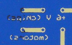
Because the artwork was flipped, the DIP chip socket no longer connects to the correct pins on the lower layer
Okay, you’ve used up transfer film, etchant, and expensive tiny drill bits. You’ve also cut boards and spent all sorts of time cleaning, ironing, etching, cleaning again, drilling, and cleaning again.
Miss anything?
The first time I did this (many years ago) I designed the whole thing on the top layer (red) even though I planned to have the circuit on the backside of the board (green).
Thinking I was smart, I simply flipped the design in the paint program before printing. Although the lettering transferred in the correct orientation, the circuit no longer matches the left-to-right pin order of the chips. If I had correctly used the PCB software, the reversed lettering on the screen would have transferred and etched in proper orientation, as well as the rest of the circuit.
Lesson: Design the circuit on the correct layers. Let the PCB software automatically handle mirroring.

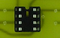
(for comparison, the GND hole isn’t drilled) Because the pads were too small compared to the hole size, the copper around some holes broke or was otherwise removed during drilling
Because I went ahead and finished the board with the mirror-image mistake in it, I learned some additional lessons before starting a fresh board.
It’s tough to line up the drill with the via holes for the through-hole components. Being slightly off can pull-up or drill-out a lot of the copper pad. This reduces the contact the solder and through-hole wire can make with the circuit. With this in mind, extend the diameter of via pads for hand drilling.
Even though I could use thinner traces (lines) for low current digital signals, I switched the entire board over to thicker traces. Since the board had the room, why not? (As long as adequate spacing exists between traces.) It saves on etchant, prevents breakage, and may improve noise tolerance.
However, don’t make the trace lines as thick as the pads or via through holes. The circles should be a little bigger than the lines they connect to, so that the solder wicks around evenly rather than heading down a line.


Left: Back side of PCB with components soldered and leads clipped. Right: Front side of PCB with components in place and top layer point-to-point wires
After mounting and soldering components, I have the first circuit board I’ve ever made!
Now I’ve got the materials (except drill bits) and I’ve learned the process.
Making reliable, repeatable printed circuit boards is much faster than point-to-point soldering. My choice of components has expanded to include surface-mounted devices with tiny pins. I can make lighter, stronger Sumo bots. I can make a line-following-robot circuit board, test it, order high-quality boards from a PCB manufacturer, a maybe make a kit for my local robot club.
My technology has made it into the 1970s. Now on to double-sided circuit boards. Or, alternatively, step up to the latest: Etching single-sided color PCBs!