

I’ve been laying out custom printed circuit boards for over ten years. There are a few tricks and tips that I use repeatedly from prototype to production PCBs to provide flexibility on parts, easier assembly, and faster circuit testing.
Most of these techniques are applicable regardless of the circuit board CAD program and manufacturer that you use.
To see the examples presented in the article, click on the file and save it.
Download Copper Connection, the PCB layout software.
Free to display, edit, and etch at home.
Linear voltage regulators are popular for their simplicity. They usually consist of three leads:
The order of the leads and the type of package (TO-220 or TO-92) varies from part to part. In the picture below, notice that none of the pinouts match.

Voltage regulator pinouts: 78L05, MCP1826, MCP1702-5002E
Sometime after the board has been made, you may find that the circuit needs a bit more current, a higher input voltage, a lower dropout voltage, or maybe you just ran out of stock of a particular voltage regulator. With a little bit of forethought, you can design your circuit board to accept a variety of regulators.

Flexible voltage regulator PCB layout
Adding a fourth and fifth hole (in this case duplicating the input and output pins) permits the following pinouts:
That covers all 6 permutations (3 factorial = 3! = 6) of pins. And, if you make sure all of the holes are 0.040 inch diameter, then you have covered both TO-220 and TO-92 packages.

Universal layout for three-pin linear voltage regulators
Small potentiometers (often called trimmers or trimpots) are also available in a variety of packages. The most common trimpots have 0.1-inch spaced leads, but the leads are attached in slightly different places with respect to the component body.

Trimpot potentiometer pinouts.
The leftmost trimpot is the least expense and doesn’t tend to twist off the board due to the staggered pins. The next trimpot is more compact, but more expensive. The next trimpot is a multiturn that can be mounted vertically or laid flat. The rightmost trimpot has a finger-friendly dial, with the non-staggered pins located at the front of the package.

Potentiometer multi-compatible PCB layout
To be compatible with all of those pinouts, you can lay out a 3×3 grid from the front of the package up through the center. All of the trimpots in the previous photograph can be dropped into that same location on the board.
On almost all through-hole potentiometers, the center pin tends to be the wiper. However, you could extend the hole pattern grid to the top of the layout in case you need to orient the potentiometer “upside down” if turning the potentiometer in a certain direction produces the opposite effect desired on the circuit.
Use three holes for capacitors, so that you can choose between 0.1 inch and 0.2 inch spaced parts at assembly time.


Extended capacitor pattern accepts capacitors with the same values but different lead spacings
For consistancy, make the first pad square and have it be positive. The other two holes are ground and are connected together.
Regardless of the size of the capacitor you insert, you always know that the first hole must be filled. The silkscreen outline also makes it understood that smaller parts should be aligned to the first hole.
An added benefit of the extra hole is that you can use it as a spare ground connection if you made a mistake somewhere else on the board.
Tactile pushbuttons are commonplace on electronic circuits due to their compact size, high reliability, and low cost. The most popular tactile pushbutton package contains four pins (for stability when pressed) and appears to be square.
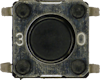
Tactile pushbutton.
In reality, the package is rectangular (slightly longer in one dimension), but you can incorrectly install it 90° out of orientation if you force the pins into the PCB holes. Normally, when pressed, the button connects one pair of pins to the other pair of pins. But, if the tactile button is installed incorrectly, it will seem as though the button is always pressed.
Before installing, you can carefully measure the continuity of the pins using a multimeter. Or, you can lay out the PCB such that the button can be installed in any orientation and still work correctly.
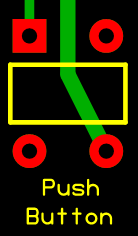
Pushbutton corner connections PCB layout
By wiring the circuit only to the pins on opposite corners, you are sure to get only one pin from one side of the switch, and another pin from the opposite side, electrically speaking. You can demonstrate this to yourself by measuring the continuity of opposite pins on a switch using a multimeter. No matter which two corner leads you select, a standard tactile pushbutton will always show continuity when pressed and no continuity when released.
You can make the pushbutton pattern more versitile by adding three extra holes in the middle.


Pushbutton pattern permits choice of parts
Now the patten can fit several types of pushbuttons or a Molex KK connector for off-board buttons.
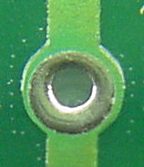
By default, most PCB layout programs use 0.056-inch diameter pads around the common 0.029-inch diameter holes. This works well for DIP chips and other closely spaced holes as there is still enough room to pass a trace between the two holes without contacting the pads.
However, in many circuit boards, most of the holes don’t have traces passing very closely -- at least not on the side of the board that the hole will be soldered. For those holes with free space around them, I always add a wider circular pad around the hole to provide a larger contact area during soldering.

Hole with larger solder pad.
In the above example, you can see the wide shiny area around the hole to ensure good solder contact between the part pin and the circuit board trace. Soldering goes faster as well, since it is easier to target the larger pad with the soldering iron tip.
A nice feature of professional circuit boards is a solder mask. A solder mask is an electrically and chemically insulating coating that protects the metal traces against the environment and unintended electrical connections.
Extended area accidentally covered by solder mask.
If you do not choose the correct element in your PCB layout program, then any extended soldering pad area that you add will get covered by solder mask during PCB production. That would eliminate the benefit of an increased surface area to solder.

Hole with circular bottom pad PCB layout
In the PCB layout sofware, make the extended soldering pad by choosing a round pad from the pad tool, rather than a circle from circle/arc tool. That way, the PCB manufacturer will not coat pads, because those are intended to be soldered. Simply move the 0.080-inch diameter pad to the 0.029-inch diameter hole to make a hole with an extended solder area.
Remember, this trick lets you have a larger soldering surface on one side of the board, while allowing traces through the pins on the other side of the board. If you need a larger soldering surface on both sides, you should simply increase the size of the pad with the hole in it.
Some parts, such as voltage regulators and motor drivers, can get hot during usage. A simple way to wick away heat is to place copper fills (large squares) under the chips. In my thermal chip tests, I demonstrate that these copper plains reduce heat and increase performance even if they are not electrically connected to the chip or the power supply.

Motor driver IC PCB layout
Of course, sometimes you'll need the area underneath the chip to run traces, and thus cannot add a copper plane. Instead, you'll see some benefits if you use thick enough traces for the chip’s power supply, and connect those traces to even small copper areas nearby.
When measuring DC voltages, it is necessary for the ground probe to be connected to the same ground as the circuit. One of the first voltages you'll measure will be the regulated power supply.
You can hunt around the board for a resistor or connector with a bare location to attach the multimeter probe. But, it can be difficult to attach probes to those locations, or that area of the board may be too crowded to access the pins.
A better solution is to add a couple of test points when you design the circuit board.

Wire loop hook test points.
Place the test points at the edge of the board to avoid wires hanging over the circuit on which you’re trying to work.

Looped wire test points PCB layout
For the loop itself, I tend to use wire cut off from component leads. Use slightly larger holes (0.035-inch diameter) so that you can use thicker wire to make the hook loops. The weight of the test probes tends to bend thinner wire.
If you place one of the positive voltage holes (+V) within 0.1 inch of one of the ground holes, and you use the larger diameter holes (0.035 inch), then you can install a Molex KK header or other similar connector as a spare power connector. That brings up the other use for these test points: spare power holes that you can wire up to correct mistakes in a circuit.
Alternatively, Nils Ove Flatjord suggests placing a large via (conductive plated through hole) near the edge of the board. Test hooks can attach without needing to solder a wire in place.

Large plated hole near the side of the PCB as a test point for a test hook
Make your ground and power traces thicker than your signal traces. Not only will the thicker traces carry more current, but the size difference makes it instantly recognizable as to which traces are for power and which are for signals. That reduces the likelihood of mistakenly hooking a power trace to a signal pin or a signal trace to a power capacitor.

Difference in trace widths reduces connection errors
I use 0.040 inch for ground/power and 0.025 inch for all other connections.
As you can see, layouts featuring a few extra holes and a little bit more copper can increase flexibility, speed installation, and improve reliability of your printed circuit boards.