

In late 1999 and early 2000, I began my self-study of digital electronics. The majority of my initial education occurred by reading and reproducing the circuits in the book Schaum’s Outline of Theory and Problems of Digital Principles by Roger L. Tokheim.
I have selected three schematics/circuits from that book to put together into a functioning project. I have chosen this particular project because it allows people to easily create something similar to my old Alphanumeric Display.
Nowadays, switch debouncing, counting, and number-to-numeric-LED-segment conversion would be done in a single microcontroller. However, you may find the stand-alone-latch-hardware-switch-debouncing circuitry to be useful in simple projects.
The first schematic is Figure 6-27 from page 127. (The three schematics from the book differ slightly from the original figures as I redrew them.)

Figure 6-27. High-level schematic of a switch, debouncing latch, counter, and numeric LED output (Roger L. Tokheim).
The total circuit consists of a single-pole double-throw switch for input, fed through a debouncing circuit, into a counter circuit, and finally into a decoder driver for display on a numeric LED. This first schematic only provides details about the input and debouncing circuitry. Later schematics go into the details of the counter and output circuitry.
The three 10 kilohm resistors provide default values (5 V) to the chip inputs if no other value is provided. You don’t need these resistors if you are going to use TTL-based chips (like a 74LS00). However, you need these resistors if you are going to use CMOS-based chips (like a 74HC00).
The input switch is a SPDT (single-pole double-throw) connected to ground (0 V).
The original schematics called for TTL (transistor-transistor logic) gates. TTL inputs interpret 0 V to 0.8 V as digital logic low. TTL inputs usually interpret disconnection (lack of current source) as digital logic high. Alternatively, the resistors provide the digital high value during switch disconnection.

Switch mechanisms that make before break (top) or break before make (bottom).
There are two ways in which a switch can be designed to act during switching. A switch can be designed to mechanically connect to the second terminal before disconnecting the first terminal (make-before-break). Or, a switch can be designed to mechanically disconnect the first terminal before connecting to the second terminal (break-before-make).
Depending on the type of switch, there are four possible switch outputs states:
| Input Switch Position | Output A | Output B |
| Up | ground = low | disconnected = high |
| Transitioning (make-before-break) | ground = low | ground = low |
| Transitioning (break-before-make) | disconnected = high | disconnected = high |
| Down | disconnected = high | ground = low |
The output signals can fluctuate considerably as a switch makes and breaks contacts. That is, the signal is not a clean, instantaneous jump from one logic level to another. Depending on the material and mechanics in the switch, either the signal flips back and forth rapidly until contact is firmly established, or a gradual voltage change occurs.
Interestingly, a gradual change in voltage will pass through the undefined voltage region on the chip inputs, resulting in a similar rapid flipping of digital logic values.
In either case, this is bad for a counting circuit!
If the input switch was connected directly to the counter circuit, the fluctuating signals would result in multiple counts per toggle. To prevent this, something needs to remove the “noise” or “bounce” from the input switch signal before it reaches the counter circuit. The debounce circuit serves this purpose.
The debounce circuit consists of an SR latch, which is also known as an SR flip-flop. S stands for set, and R stands for reset. (Technically, since it is made from NAND gates, it is actually “not set” and “not reset”.) Because the gates in the latch feed outputs back into inputs, the SR latch can be complicated to analyze.
A simple way to begin the analysis is with the operation of a standalone NAND gate.
| Input A | Input B | Output Y |
| Low | Low | High |
| Low | High | High |
| High | Low | High |
| High | High | Low |
The table shows that if either of the inputs is low, the output is always high. This is a very useful rule for unraveling the SR latch, because if one of the inputs if low, we don’t need to know the other input value to that gate in order to determine the output.
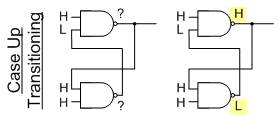
When the input switch is in the up position, a low signal and a high signal are fed into the SR latch debounce circuit. Since the output value of a NAND gate is always high when at least one input is low, that result can be followed through the rest of the circuit to determine the final result.
In the figure below, each new result is highlighted in yellow. 'L' is low, 'H' is high, 'x' is don’t care, and '?' is unknown.

Output of the debounce circuit when the input switch is in the up position.
On the left side of the figure, only two of the inputs are known (the ones coming from the switch). The outputs are unknown. Then, going from left to right, an output is solved (H), which is connected to an input (H), which causes the gate to output (L), which solves our last input (L).
Therefore, when the input switch is in the up position, the debounce circuit output is high.
The same analysis technique is applied for the down position.

Output of debounce circuit when the input switch is in the down position.
When the input switch is in the down position, the debounce circuit output is low.
The real usefulness of the SR latch comes during input switch transitions. Let’s assume the input switch is a break-before-make and the switch starts in the up position.
From the prior analysis, the inputs values when the switch is up are low, low, high, high, and the output is high. As the switch is toggled, it breaks the first input, changing it to high, low, high, high. Those values can be used to determine the output value.
Output of the debounce circuit when the input switch is starting to be toggled away from the up position.
When the input switch changes from the up position to the center position, the debounce circuit output remains high. It is unchanged from the up position!
This means that even if the input switch signal bounces multiple times between low and high signals as it breaks the connection, the debounce output remains steady. Because the debounce output is steady, the counter doesn’t increment spuriously.
Not surprisingly, the same steadiness occurs when the input switch starts in the down position and starts to break contact as it transitions up. The output remains low.

Output of the debounce circuit when the input switch is starting to be toggled away from the down position.
While this is exactly what we want, this also explains why a single-throw switch or pushbutton won’t work. This circuit keeps the output in a steady state when only one input is changing back and forth. Pushbuttons and single-throw switches only change one input.
Double-throw switches provide more information. By requiring two inputs to change states, not just one, you can ignore all errors generated by either input at a given time. You don’t care how long it takes for the errors (bouncing) to go away, but you’re ready to change states again right away if necessary.
Software debouncing of pushbuttons relies on time as the second input. That is, the software assumes it takes a certain amount of time for the switch to settle down before more input can be reliably accepted. This slows down the maximum switching rate and the software method is still vulnerable to long bounces.
In the previous two examples, it was assumed that the switch is a break-before-make type of switch. Instead, if the switch is make-before-break type, the switch will output two low values into the SR latch.

Make-before-break switch always causes a high output in this circuit.
A low input into a two-input NAND gates always results in a high output, regardless of the other input value into that gate. As such, it doesn’t matter what the prior state of the SR latch was, the make-before-break input switch will always result in the debounce circuit outputting high during input switch transitions.
This is undesirable behavior when toggling from the down position, as the bouncing will flip the input to the counter between low and high, causing extra counts. Therefore, the switch must be break-before-make double-throw, not make-before-break.
Admittedly, this further reduces the occasions when the circuit may be useful to you. However, this is a limitation of using only two logic gates. In a microcontroller, you can write a slightly more complex algorithm that will work with either type of double-throw switch:
			1. Output Y=low // Default at power up

			2. If Input A=low  and Input B=high then Output Y=high; Goto 4

			3. Goto 2 // Low output unless the switch is in the full up position (L H)

			4. If Input A=high and Input B=low  then Goto 1

			5. Goto 4 // High output unless switch is in the full down position (H L)
There is one last pair of cases to consider that are classic for an SR latch. If a break-before-make switch is in the center position (neither up nor down) during power up, what is the output?
From the prior analysis of the up and down transition states, we know that the SR latch will remain stable in its prior output state. If the individual NAND gate outputs happen to power up as either “high, low” or “low, high”, they will remain that way (because that’s identical to the already analyzed up/down transition states). But what if the individual NAND gate outputs initially power up as “high, high” or “low, low”, feeding those value into the center inputs of the SR latch circuit?

Oscillating states for an SR latch at power up.
Theoretically, the SR latch will repeatedly oscillate between a high output and a low output. In reality, the slight differences between transistors will cause one output to trip slightly sooner, causing the center inputs to no longer match each other, causing the circuit to stabilize.
Again, an oscillation can only happen if the switch is neither up or down at power up.
According to the first schematic in the book, after the input switch signal is debounced and pulled-up (if necessary), it is fed into a counter. Because the first schematic does not provide any details as to the counter circuit, I selected the schematic in Figure 10-20 on page 249.

Figure 10-20. A decade (mod-10) counter circuit (Roger L. Tokheim).
The 74HC393 is not a “TTL” decade counter as described in the first schematic. Rather, it is a “CMOS”-based decade counter. Fortunately, the pull-up resistor in the first schematic allows the families to be interfaced. Alternatively, a TTL chip (like the 74393) can be substituted in this second schematic.
The counter chip produces a binary output in the 8s, 4s, 2s, and 1s place based on the number of pulses counted from the debounced input switch signal. The signal feeds into the clock input on the counter.
The output on this counter chip provides a range of 16 values (0-15). However, since the output of the numeric LED can only display values 0-9, the counter output range needs to be constrained.
The count is limited by the AND gate at the bottom of the schematic. The AND gate receives the outputs of the 8s place and the 2s place. When both 8 and 2 are high in the output, the count must be 10 or greater. When both of the inputs to the AND gate are high, the AND gate outputs a high signal to the master reset pin on the counter chip to start the count over at 0.
The 7400 NAND chip contains four NAND gates. Only two of the gates are used in the debounce circuit. It seems a shame to add a whole AND chip and waste the two remaining NAND gates. So, when this project was actually implemented, I substituted the two NAND gates for the AND gate.

An AND gate can be made from two NAND gates.
The final part needed to complete the project is an output circuit. An appropriate schematic is Figure 7-13 on page 150 of the book.

Figure 7-13. Wiring of decoder and seven-segment LED display. (Roger L. Tokheim)
The output of the counter circuit is fed into a decoder chip designed for generating human-readable numbers on a 7-segment LED. The output of the decoder chip passes through 150 ohm resistors to limit the current drawn to a safe and consistent level.
The term “common anode” refers to the fact that the anode portions of each LED segment are connected together at the upper voltage source. This means that individual LED segments are lit by connecting their cathode to a lower voltage. Although it seems backwards to turn on the LED segments with a low signal, early logic chips like standard TTL are capable of delivering a greater amount of current with an output that is logic low.
To complete the project, I implemented it on a solderless breadboard using a 74F00 (for debouncing), 74LS393 (for counting), and 7447 (for LED display). Since I’m accustomed to CMOS chips, I chose TTL chips to try something different. No pullup resisters were used.
The 5V power source is located externally.

Implementation of the Switch Counter Numeric Display (click to enlarge).
At first, the circuit skipped numbers and reset somewhat randomly. The reason is that standard TTL chips consume a lot of power and generate a lot of electrical noise during switching.
From my previous experience with digital circuitry, I realized that adding small bypass/decoupling capacitors to each chip and bulk capacitors (see Chapter 8 of Intermediate Robot Building) on the power rails would correct the situation.
The finished circuit works very well.