

How much larger should the PCB hole be than the part? A rule of thumb is that you should make a PCB hole 0.007 inches larger than the part lead diameter.
For example, if you have a resistor with a 0.022 inch lead diameter, the hole diameter should be at least 0.029 inch.
Wait a minute! If you have a 0.022 inch part, why not a 0.022 inch hole? Well, manufacturing isn’t perfect. On the datasheet for the part, you will find a tolerance specified with plus/minus some amount to compensate for variations in machining, material, plating, temperature, wear, aging, and so forth.
For example, the datasheet for a specific manufacturer of 1/4-watt resistors says the lead diameter is 0.022 ±0.003.

Resistor datasheet specifying diameter tolerance
Simply subtract the tolerance from the standard value to find the minimum, and add the tolerance to the standard value to find the maximum. Therefore, the actual part can vary from 0.019 to 0.025.
In practice, you will find most of the parts are fairly close to 0.022. Occasionally, you’ll find a part that is outside of the specified range, which would be considered a defective part because it didn’t meet specifications.
Okay, if the resistor can only be as large as 0.025 inch, why make the hole 0.029? Ahh -- because the hole has tolerances, too!
As each hole is drilled, the drill bit wears down a little bit. Alternatively, the drill may wiggle or vibrate slightly in a hole, causing a slightly oversized hole. After that, the hole is plated. The plating may be slightly thicker or thinner for each batch or position on the board. You also have to account for thermal expansion or shrinkage of the PCB substrate as it is being processed.
Many PCB manufacturers specify a hole tolerance of ±0.004. So, 0.022 resistor lead + 0.003 resistor lead tolerance + 0.004 PCB hole tolerance = 0.029 inches.
The 0.007 inch rule of thumb is adequate for hobbyists and prototyping most of the time. Of course, it is better to check out the datasheets and online specifications for the part and PCB manufacturer you will be using. Often, the specified tolerance will vary based on hole size and type of plating. In fact, professional designers also take into account the type of solder and the soldering process.
If you design enough PCBs, you’ll eventually make the mistake of choosing too small of a hole.
I’m embarrassed to admit that I ordered $150 dollars worth of boards without any tolerance on the resistor hole sizes. The resistors did not fit. As a workaround, I sorted my resistors to find those with the skinniest leads in their batch. Even then, a few of the PCB holes needed to be enlarged by hand with a jewelers drill (aka pin vise).
A more complicated example came from a reader. He had been using ExpressPCB as a manufacturer, but switched to OSH Park. He discovered that one of the parts no longer fit in the hole. Was it a bug? Was it a manufacturing mistake by OSH Park? It turns out it was neither. It was a tolerance issue.
He sent me his PCB source file and uploaded photographs of the boards. How could I accurately measure the actual hole sizes from a couple of photos? Adding to difficulty, some minor changes had been made to the board layout.
I began with a screenshot of the source layout. In Microsoft Visio, I drew orange lines to indicate significant locations on the layout (text top/bottom and center of holes). I then proportionally resized the photos of the boards until the lines matched. At that point, I knew the source and photos were all scaled equally relative to each other.
On the source layout, I outlined the holes with blue circles. Without changing the size of the circles, I copied them to the photos to make it easy to see the difference between specified hole size and actual hole size.

Determining hole size from photos
Although this methodology is too crude for absolute measurements, it suggests:
Back to the problem at hand: Why didn’t his part fit anymore?
It turns out, the manufacturer of the part actually recommends a 0.043 inch hole (not 0.033), and ExpressPCB’s choice of a larger drill bit was providing just enough room for the error to be overlooked. By subsequently using the recommended hole size, he was able to have the boards manufactured wherever he wanted.
This brings up an interesting question, how good are PCB manufacturers at actually meeting their specified tolerances? Established manufacturers work very hard to do so, because they don’t want to pay the high cost of scrapping boards when a customer discovers a problem.
How can I check this myself?
My first thought was to take high-quality photographs of various boards and have the computer analyze hole size variance. Unfortunately, the angle of the camera to each hole is different. Thus, holes on the far left and far right sides of the board appear narrower due to the visibility of a side.

No big deal. I’ll just use a flatbed scanner.

Are you kidding me? I thought a flatbed scanner used a really long row of photosensors -- similar to old fax machines. Instead, I learned that a consumer flatbed scanner uses a curved mirror and a camera. So, the angular effect still occurs.
Worse still, the object is lit from only one direction, causing a pronounced shadow. Better quality scanners might be lit from above and below, but maybe not, since most scanned objects are flat like paper.
Although I’m sure there are high-end tools for optically measuring hole size and roundness, there is a relatively inexpensive manual method. A pin gage (not pin gauge), consists of a box of precision metal rods sorted by diameter.
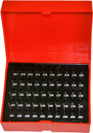

Shars pin gage set 303 4501
You simply insert the pin into the hole and determine if it fits. If it does, choose a larger size until you find a pin that doesn’t fit.

Measuring PCB hole size with pin gage
Of course, tolerance appears again. There is no such thing a perfect pin gage set. The Shars 303-4501P set has a tolerance of ±0.0002. Not 0.002 (two thousandths) but 0.0002 (two ten-thousandths). That’s more than enough for this test.
I tested eight double-sided boards for two hole sizes: 0.125 inch and 0.29 inch.
| Manufacturer | Year | Notes | 0.125 Diameter Holes | 0.029 Diameter Holes |
| ExpressPCB | 2001 | no silkscreen or soldermask | ⌀0.125 ×1 ⌀0.126 ×3 | ⌀0.029 ×14 |
| ExpressPCB | 2002 | ⌀0.124 ×3 ⌀0.125 ×1 | ⌀0.029 ×13 ⌀0.030 ×1 | |
| ExpressPCB | 2011 | ⌀0.125 ×4 | ⌀0.029 ×4 ⌀0.030 ×10 | |
| ExpressPCB | 2011 | silver has oxidized | ⌀0.128 ×4 | ⌀0.031 ×14 |
| Advanced Circuits | 2012 | ⌀0.122 ×1 ⌀0.123 ×3 | ⌀0.028 ×14 | |
| Electronic Interconnect | 2013 | ⌀0.123 ×1 ⌀0.124 ×3 | ⌀0.029 ×4 ⌀0.030 ×10 | |
| Electronic Interconnect | 2013 | blue solder mask | ⌀0.125 ×4 | ⌀0.028 ×14 |
| OSH Park | 2015 | gold wash | ⌀0.126 ×3 ⌀0.127 ×1 | ⌀0.029 ×14 |
I conclude that all of these manufacturers met the tolerances specified. You should anticipate variances of at least ± 0.003 in PCB hole sizes.
In the above table, notice one board is listed as “silver has oxidized”. Some time ago, ExpressPCB had a lead-free silver finish that oxidizes when exposed to air. Compared with their standard finish at the time, that board is now crusty and unsolderable without treatment.
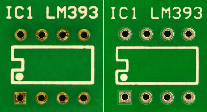
Comparison of dip hole pattern with different finishes
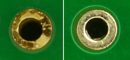
Lead free silver plating has oxidized compared to leaded finish
In summary, always remember to use a hole size that is at least 0.007 inches (0.2 millimeters) larger than the diameter of the leads on the part you want to insert. If at all possible, refer to the datasheet to find the manufacturer’s recommended hole size.
I found that established PCB manufacturers are good about meeting their published tolerances, but you should expect that most holes will not be exactly what you specify.